In-depth Analysis of Pogo Pin Contact Impedance: Influencing Factors and Material Optimization Strategies
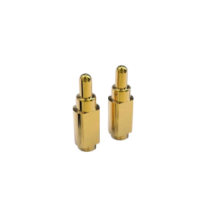
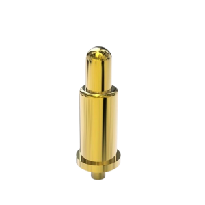
Our test data shows that achieving a calculated, predictable Pogo Pin contact impedance matrix is a vital baseline for engineering high-speed data telemetry, high-frequency RF connections, and high-amperage power rail distribution. We engineered our spring-loaded terminals to resolve the persistent industry bottleneck of unstable, erratic resistance drift during high-cycle equipment lifecycles. By matching precision-machined C3604 Brass barrels with calibrated 3u” Gold plating, our terminals maintain a highly stable, low-profile contact resistance profile below <30mΩ across 100,000 continuous compression cycles. This mechanical integrity directly prevents signal loss and voltage cutoffs, outperforming generic low-end connectors that face catastrophic plating wear and resistance inflation after fewer than 5,000 cycles.
I. Comprehensive Components of Pogo Pin Contact Impedance
To systematically optimize component connection points, hardware engineers must evaluate the three distinct physical layers that dictate cumulative circuit impedance grids:
- (I) Concentrated Resistance: Microscopically, the mating face between a spring plunger needle and a landing pad is a cluster of minute physical contact spots (a-spots). As current forces through these constricted paths, the localized current lines contract, amplifying localized current density and yielding concentrated resistance. Utilizing our highly conductive base alloys reduces this localized restriction immediately.
- (II) Film Resistance: Surface film resistance is caused by dense oxide layers or loose environmental dust particles settling on the terminal tip. We utilize stable metallurgical surface treatments to block rapid oxidation without compromising the main electrical path.
- (III) Conductor Resistance: Measured from the contact lead tail directly through the component body, conductor resistance is dictated by the native resistivity of the turned brass housing and is subject to thermal shifts. According to linear copper/brass temperature coefficients, active operation under elevated thermal conditions inflates conductor resistance, requiring robust dissipation design.
II. Critical Factors Driving Pogo Pin Contact Resistance Fluctuation
1. Plating Wear and Atmospheric Oxidation Layers
Exposed metal surfaces develop dense micro-thin oxide films within hours of atmospheric exposure. Under continuous mating friction, generic connectors with thin “Gold Flash” coatings under <0.1u” quickly expose raw copper base alloys to moisture corrosion, resulting in steep, uncontrollable impedance spikes over time.
2. Pre-Loaded Spring Force and Contact Geometry Style
A weak internal spring cannot generate sufficient mechanical force to slice through surface flux residues or OSP films on the mating PCB pads. Conversely, excessive spring pressure induces early plating scoring and terminal distortion. We engineer precision-wound SUS304 or Beryllium Copper (Be-Cu) internal springs to maintain a continuous, uncompromised 60g to 120g load center, ensuring clean mechanical wiping actions even under intense transport vibration environments.
III. Standard Technical Specifications: Verified Operational Parameters
For high-speed Bill-of-Materials (BOM) auditing, hardware specifiers can directly cross-reference our verified operational parameters against standard legacy averages:
| Key Impedance Parameter Group | Jiatel High-Reliability Specification | Low-End Competitor Average |
|---|---|---|
| Initial Contact Resistance | ≤ 30 mΩ Baseline Threshold | ≤ 50 mΩ (Volatile across batches) |
| Impedance Delta (Post 100k Cycles) | ΔR ≤ 20 mΩ (Locked low-drift window) | Fails entirely or drifts past >200 mΩ |
| Standard Terminal Plating | 3u” Hard Gold (Au) over Nickel | <0.1u” Gold Flash (Rapid wear profile) |
| Internal Spring Metallurgy | SUS304 Stainless / Beryllium Copper | High-Carbon Steel (Prone to rust and fatigue) |
IV. Industrial Customization and Supply Chain Velocity
We operate integrated automated intelligent manufacturing lines and vertical production systems to adjust internal needle dimensions and plunger angles. Whether your design requires custom 2.5mm pitch 2-pin arrays, 3-pin spring terminals, or high-density custom multi-pin blocks for 5G telematics, our engineering team supplies a comprehensive 12-hour DFM analysis to match your targeted impedance specifications while keeping tooling MOQs highly accessible.
V. Audited Drawing Vault & NPI Engineering Queue
High-speed data transmission grids demand absolute mechanical coplanarity and flawless footprint pad validation. To enforce strict version control and isolate our clients from board routing faults, we restrict uncalibrated public 3D layout downloads. Our Senior NPI Engineering Team distributes mass-production-ready drawings directly instead.
If your project faces erratic resistance hurdles or requires strict 1:1 drop-in cross-references to replace costly legacy brand connector layouts, route your spatial clearance boundaries and current parameters directly to our engineering queue for review:
SLA Delivery Commitment: We officially guarantee that checked, production-ready [Technical Datasheets] and [2D Footprint Specs] will be dispatched in verified PDF format within 12 hours after registration in our NPI Engineering Queue.